Every chip that powers AI, smartphones, autonomous vehicles, or data centers begins long before it reaches silicon. Behind every successful semiconductor lies a carefully orchestrated design flow that transforms an idea into a manufacturable chip.
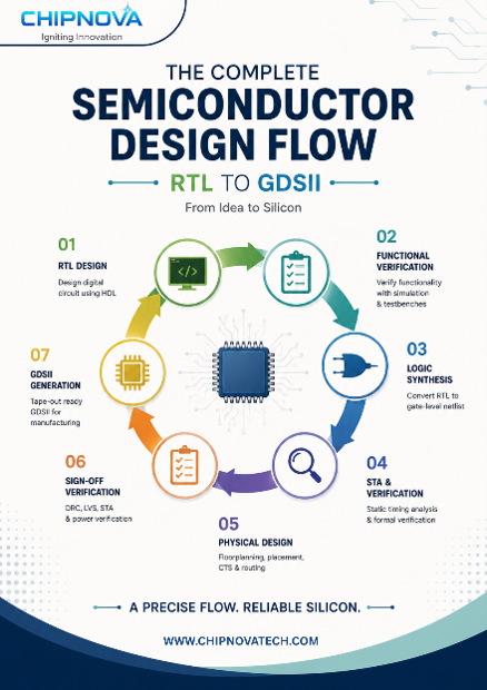
The journey starts with RTL (Register Transfer Level) Design, where engineers define the chip’s functionality using hardware description languages such as Verilog or SystemVerilog. This is followed by Functional Verification, ensuring the design behaves exactly as intended before moving forward.
Once verified, the design progresses through Logic Synthesis, converting RTL into a gate-level netlist, followed by Physical Design, where floorplanning, placement, clock tree synthesis, and routing bring the design closer to reality. Finally, rigorous sign-off verification confirms timing, power, and manufacturability before generating the GDSII file; the blueprint sent to the fabrication facility.
Each stage plays a critical role in reducing design risk, improving performance, and achieving first-time-right silicon. As semiconductor technologies continue to evolve, success depends not only on innovation but also on a disciplined design methodology and rigorous verification at every step.
At Chipnova Technologies, we help engineering teams deliver reliable semiconductor solutions by supporting every stage of the RTL-to-GDSII journey.